bill of materials (BOM):
shopping:
- for your convenience, here’s a mouser cart (2d, 2e). note — this has 20mm D-shaft encoders, black button caps, and includes the teensy 3.2 (which can be had cheaper at oshpark)
- the cart doesn’t include:
- machine-pin headers/sockets (for mounting the teensy dev-board).
- thonkiconn jacks.
- 1.3” OLED display.
- (note: if you prefer, you can use standard (square) sockets/pin headers, but not all of them will fit the PCB. these come with a small enough pin-diameter, for instance; as do these.)
- re knobs: options include sifam (w/ “encoder caps”), rogan 2s, and cliff K85 (+ suitable cap).
panels:
- current options include: DIY (.fpd, .svg), common ground/KOMA, grayscale, magpie, and oscillosaurus.
schematic:
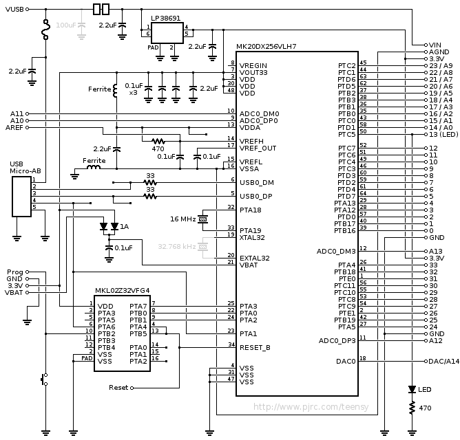
- see here (2e) (2d, 2c is basically identical)
board revision change log:
- see here (check in case of doubt)
component overlay:
troubleshooting:
notes:
-
make sure to take a look at the note re: OLED below.
-
NB: versions prior to 2e:
-
1) with the exception of the four 75k resistors (which go where it says 49k9), and the four 560p caps (which should go where it says 10n), you can follow the values printed on the board. no special precautions required otherwise.
-
2) ignore the 3-pin header adjacent to the 2x14 teensy header, it’s not needed; neither is the SOT-23 part labelled LM4040-2.5 (top side). Q is where the four NPN transistors go.
-
3) as noted in the BOM, it’s preferable to use 0.1% resistors, not 2k trimpots for the output stage (= the stuff around the dual op amps) (that’s irrespective of the version of the board that you might have). ditto for the input stage, don’t use the trimpot, but 75k resistors.
-
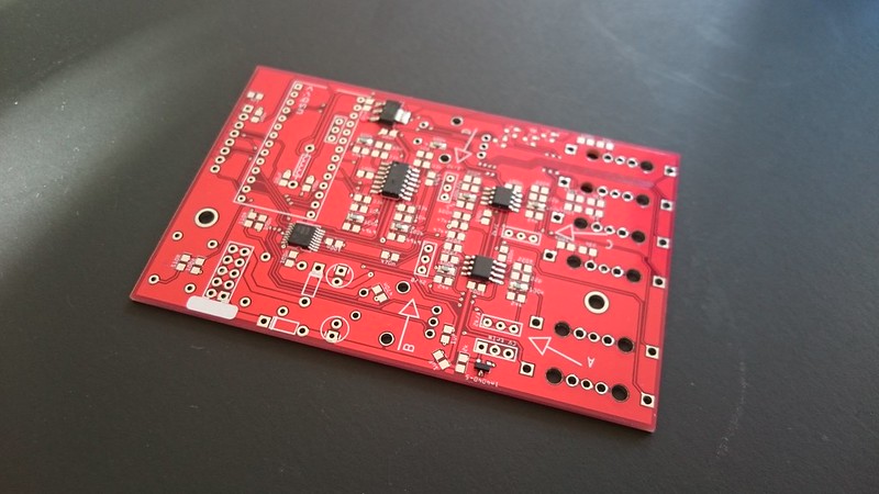
populating the board:
typically, you’d do the ICs first:
- be careful with the orientation of the OPA2172s: white dot = pin 1:
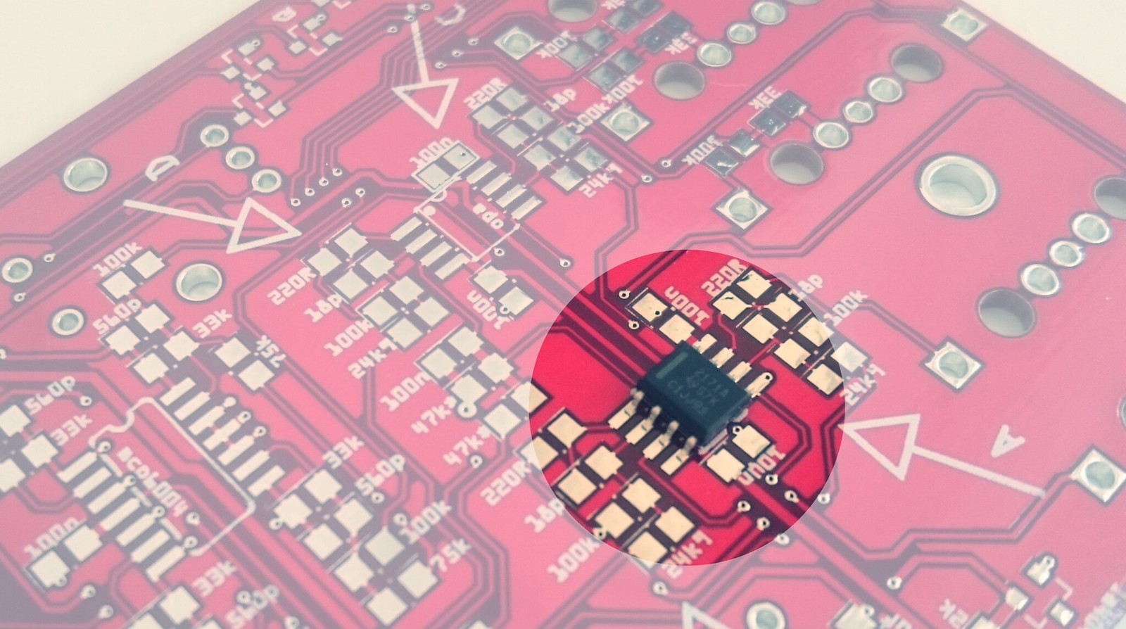
- that’s also where the 0.1% resistors should go — the
100k(0.1%) ones are the ones in parallel to24k9.
… followed by the passives:
- note: use 75k where it says 49k9! and ideally, 560p or less where it says 10n. (if it says so, silkscreen fixed in 2e)
- (and don’t forget the ADP150 and passives on the top side of the board!)
… followed by the through-hole and mechanical parts:
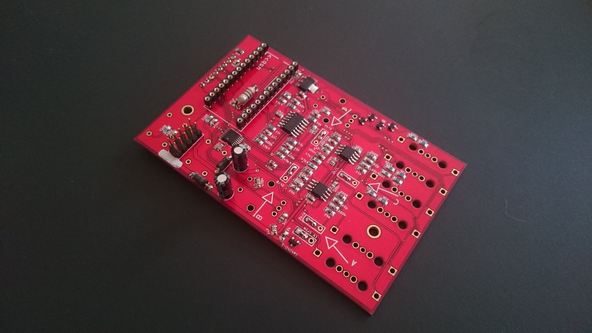
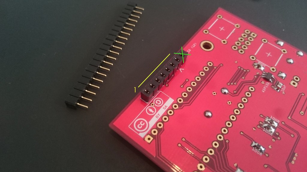
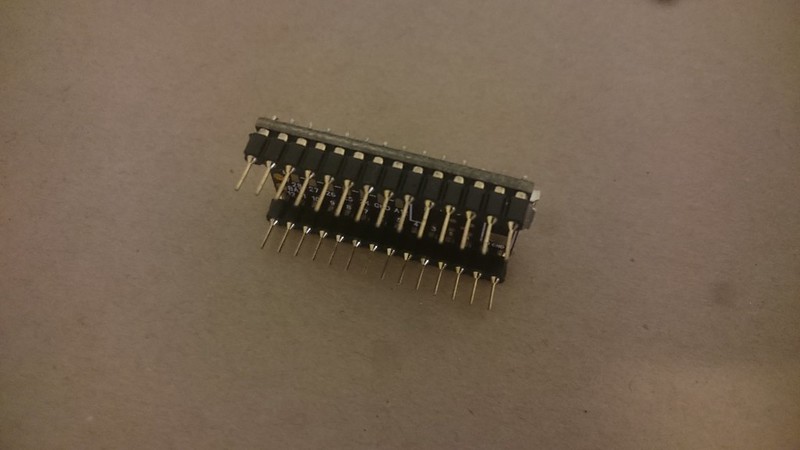
- inductor, 2x5 header, 22uF caps, diodes, sockets for teensy and the OLED.
- note: 2x14 sockets w/ round pins (as pictured): because the PCB holes are small.
- 1x7 (or 1x8) socket for the OLED: standard square holes, but low profile:
- use either a 7 or 8 pin header, the OLED goes between the square pin (pin 1) and the one marked with
^(pin 7); the rightmost signal (pin 8 = teensy pin 12) is unused.
NB: … jumpers (2d and earlier):
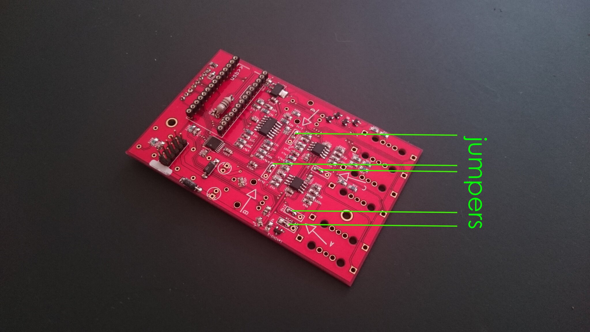
- note the five jumpers across the 3-pin pads! (the gaps in question should be easily visible).
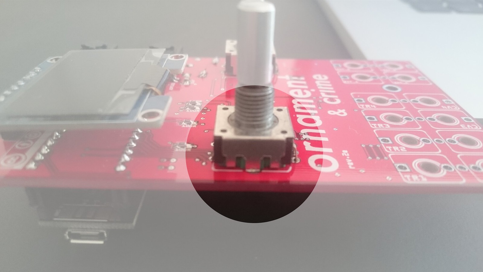
encoders:
- you’ll need to bend the lugs inwards slightly, then they’ll fit snugly:
- NB: previous PCB revisions had holes that were too small for the lugs — in case you have such a PCB, just snip off the lugs:
- either way you’ll need a bunch of washers so that things line up nicely. also keep in mind that the threaded part is finite, so the preferred solution will somewhat depend on choice of encoder and panel thickness. (especially when using 15mm encoders, it might make more sense to actually solder the encoders onto the top side of the board, leaving some space between the PCB and the body of the encoder).
jacks:
- the jacks share the ground pad, facing each other:
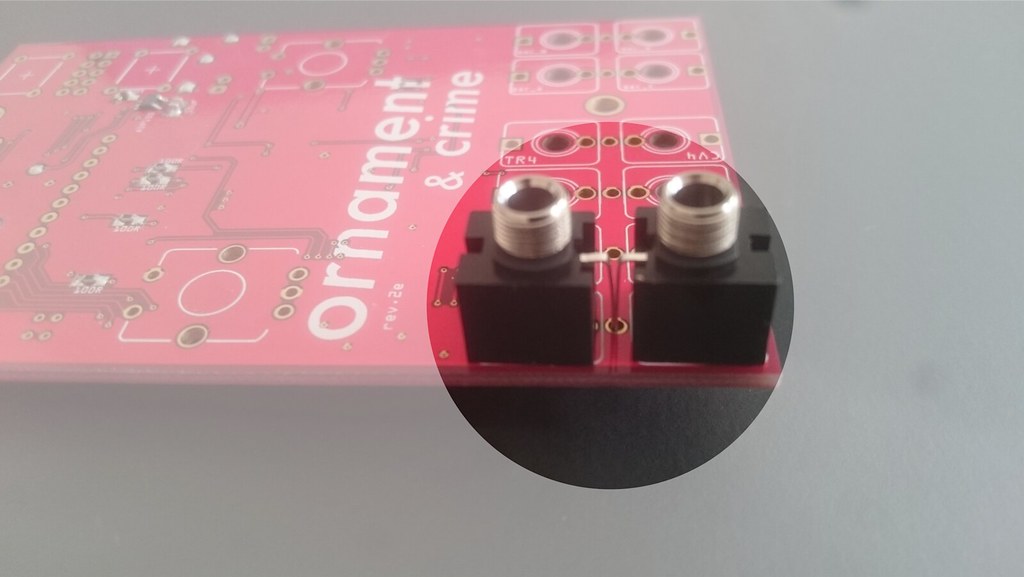
- to properly align the jacks, it’ll make sense to fit the panel first, only then solder them to the PCB.
OLED
-
the OLED (7 pins) goes between pin 1 (ground) and the
^mark: ignore the right-most signal (pin 8), that’s DIN/MISO, which isn’t needed for the display. -
before inserting the display, make sure that the OLED is configured for SPI (see the resistors/labels on the back side of the OLED — there’s a slim chance it’s configured for “i2c”, which wouldn’t work).
-
if using an aluminium panel, also make sure that the OLED-pins (top side) don’t touch the panel! — cut them flush with the carrier-PCB (and best to insulate the panel with a piece of tape).
-
also: as per the BOM, use a low-profile socket! — you’ll have to trim the OLED-pins (bottom side) to approx. half their length (or replace them, if you’re adventurous) so as to make things fit / line up with the other components (ie jacks, encoders):
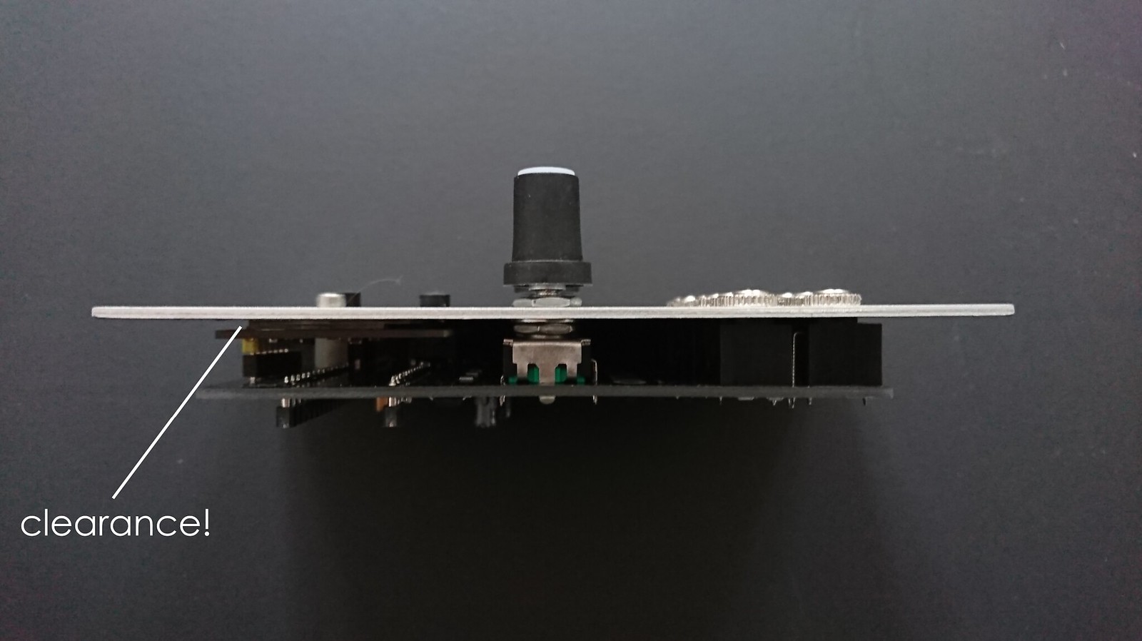
- if your OLED refuses to sit properly, a suitably sized spacer (~ 6mm) will help:
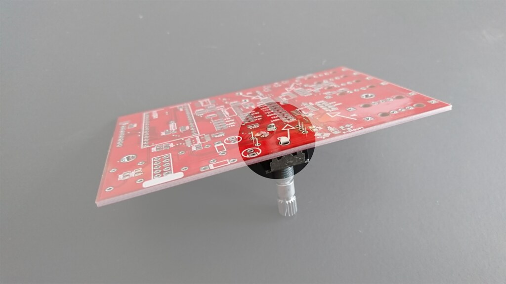
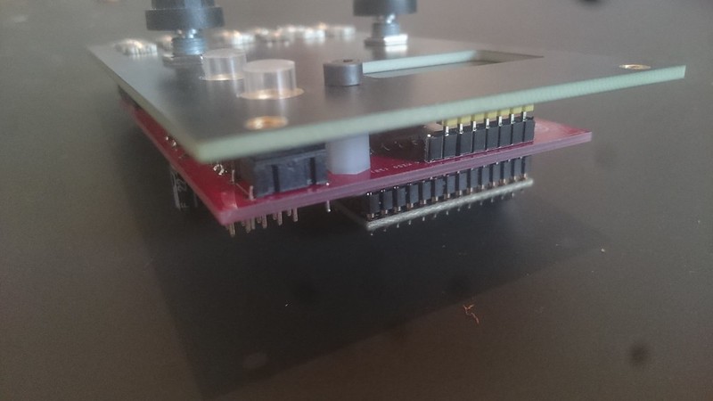
spacer:
- the spacer (10mm, ⌀ 3M) goes right next to the tactile buttons:
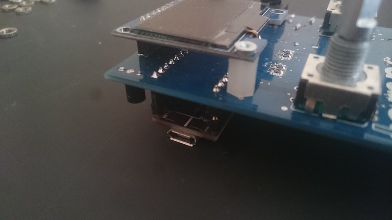
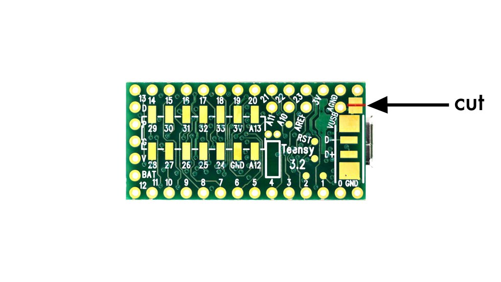
finally. prepare + insert the teensy:
- you have to cut one trace (†):
- and solder the pin headers, which look like so:
done.
- before inserting the teensy, it’ll make sense to check some basic things, first. here’s a few points to test:
(†) (note):
- cutting the trace is mainly a precautionary measure — it is to prevent people (you) from powering the teensy dev-board simultaneously from USB and the eurorack PSU when updating the firmware (or when “debugging” code via serial USB); doing so might have undesirable consequences. see the T3.2 schematic for details.
- cutting the trace is not essential for the module to work. if you prefer, you can leave the trace intact as long as you remember to disconnect your module from the eurorack PSU when connecting a/the USB cable. in this case, the teensy will be (= must be) powered solely from V_USB (= 5V) via the USB-cable, which will be just as fine for the purpose of occasionally flashing the MCU.
- Corollary: Note that if you do cut the V_USB trace, of course you then won’t be able to upload the firmware unless you power the teensy 3.2 by way of powering up the module.
trouble-shooting
-
if things don’t work out as expected/intended, here’s a few things that you might want to check:
- if you’ve used a panel made from conducting material (e.g. aluminium), do the OLED pins touch the panel?
- op-amps oriented correctly? (see the pic and component overlay)
- any solder bridges or loose contacts? (reflow tricky parts, just to make sure).
- forgot to solder the components on the top side of the board (ADP150 etc)?
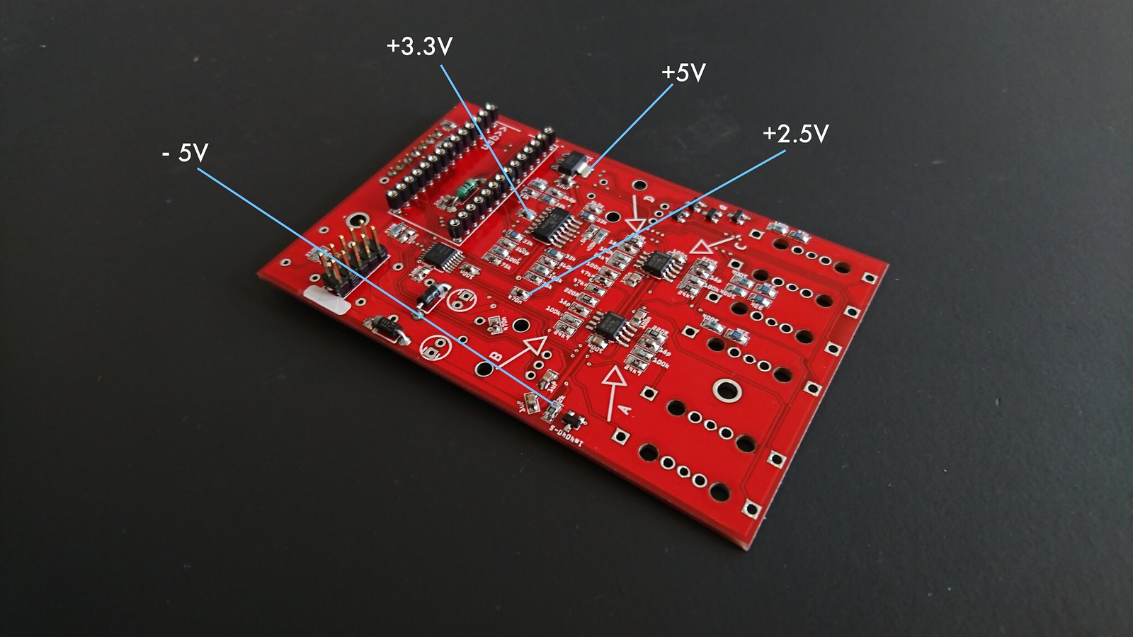
- power rails and reference voltages doing ok? — see above and below.
-
common symptoms include:
- outputs aren’t working and the 2.5V reference voltage is not present (see here): in this case, chances are something is amiss with the DAC. double check its orientation, supply voltage (3V3_A, via ADP150), and reflow the DAC pins.
- all outputs are stuck at ~ 6.25V: in this case, communication with the DAC typically isn’t working properly. double check (reflow) the SPI signals from the teensy to the DAC; that’s DAC pins 9, 10, 11 in particular (also double-check DAC pins 13 - 16).
- only some of the outputs work properly: in this case, chances are something’s off with the output stage (corresponding to the misbehaving channel). check the dual op-amps and surrounding passives.
- the DAC seems to work (in principle), but calibration points > 0V cannot be tuned properly / are way off: in this case, typically one of the outputs is shorted into 0V. check the jacks for shorts.
- some or all of the CV inputs aren’t working correctly: to further diagnose, there’s a debug menu which can be entered by long-pressing the right encoder (= enter app selection menu), and then clicking the left encoder. hit the left encoder three times to go to the ADC debug page, which shows the raw ADC values:
- with no signals patched, the rightmost column should show a value of ca. ~
2730for all four inputs: that’s the voltage offset at the ADC pins (which should be: 2.2V =~ 2/3 * 3.3V < > 2730 =~ 2/3 * 4096 ). - if none of the channels shows a value of ~
2730, most likely there is no -5V offset: check the LM4040 is working properly/actually outputting -5V; also check the 100R resistors on the top side of the PCB (forgot them? used 100k instead of 100R?); lastly, check the MCP6004: is this ok / working properly otherwise? - if only some of the channels don’t show a value of ~
2730, check the 75k resistors. - if the offsets are all ok (all channels showing ~
2730), but individual CV channels don’t register a signal, check the 100k (input) resistors.
- with no signals patched, the rightmost column should show a value of ca. ~
- some of clock inputs aren’t working: check the four transistors and associated passives (in the lower right half of the PCB/where it says Q).
- clock input
TR3isn’t working; if you’re positive the transistor is ok: there’s a via fairly close to the teensy VIN pin and the 10uF cap nearby. double-check there’s no short there. - the module seems to work fine (outputs etc), but the OLED display isn’t working — double-check that your 1.3”/7-pin OLED is set up for SPI. (check the resistors/labels on the back side of the OLED.)
Video of building an Ornament & Crime
- a nicely produced, entertaining and informative review - essential viewing for anyone contemplating building an Ornament & Crime