in brief
- Teensy 3.1 / 3.2 dev board (Freescale MK20DX256 / 32-bit ARM Cortex M4).
- 4x precision CV outputs, 16-bit (TI DAC8565).
- output range: -3v/+6v, “in-the-loop” compensated, for proper DC accuracy (+ 9 calibration points per channel, settable in firmware); +/- 0.2mV error across a 9 octave pitch CV range is achievable.
- 4x CV inputs, -3.5v/+6.5v, 12bit, 100k input impedance.
- 4x trigger/gate inputs, threshold ~ 2.5v, > 100k input impedance.
- two rotary encoders, with built-in push switches.
- two push buttons.
- 128 x 64 pixel 1.3” OLED display (SPI / SH1106 driver chip).
- trigger-to-quantised-output latency < 100 microseconds.
- 16.67kHz internal timer (CPU overclocked to 120MHz), which is also the DAC update rate. ADC samples are acquired (via DMA) at ~ 5.55kHz but in several of the o_C “apps”, values are further averaged to remove noise, meaning that the effective sample rate for CV inputs is about 1kHz. Digital (gate/trigger) inputs are read at 16.67 KHz — this ensures very low latency.
- +/-12V power only, ca. 85mA power draw on +12V bus, < 10mA on -12V bus)
more verbose
-
o_C is a fairly straightforward DAC breakout board for the teensy 3.1/3.2 ARM development board (cortex M4), with an OLED display: somewhat like a pimped-up “ardcore”, though its focus is on generating precision control voltages rather than being (entirely) general purpose (see the schematic and note re SPI below).
-
to this end, the board features four 16-bit CV outputs, courtesy of DAC8565. The outputs (range: -3V/+6V) are “in-the-loop” compensated to ensure proper DC accuracy, ie. to prevent any voltage errors when connected to (the usual) 100k input impedances downstream. with suitable equipment, it’s feasible to tune the calibration points (9 per channel) accurate to +/- 0.0002V; ie tracking shouldn’t be half-bad, at all (that’s an error for pitch CVs of well under 1 cent, where a cent is one-hundredth of a standard semitone (1200 cents per octave) — the limit of human pitch difference detection is about 4 cents, thus the pitch CV tracking in O+C can be calibrated to be more accurate than your ear, or your VCOs).
-
in addition, there are four CV inputs (~12 bit, -3V/+6V range, 100k input impedance) as well as four digital inputs (> 100k input impedance, threshold ~ 2.5V), two encoders (w/ switch), and two tact switches.
-
as the DAC shares the SPI port with the 128x64 OLED display (teensy 3.1/3.2 only has one such port), the thing is not really suitable for applications that need to write to the DAC at audio sample rates (ie VCOs etc). that said, with some DMA trickery, and pld’s custom interleaved OLED/DAC driver (which is included in the ornament & crime firmware), the DAC update rate is 16.67kHz per channel.
-
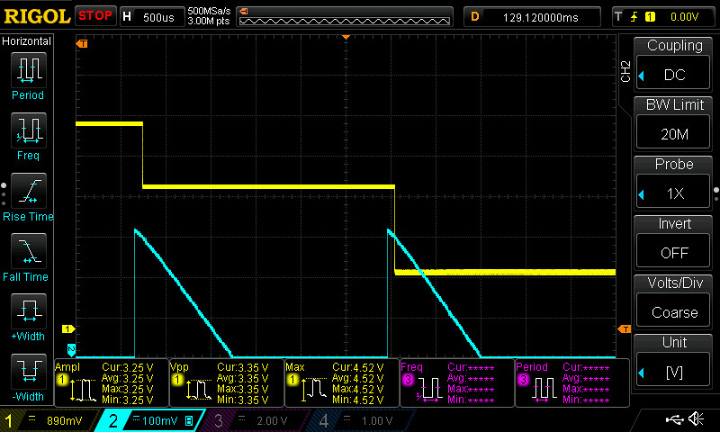
the trigger-to-quantized-output latency is pretty decent (< 100us), too:
-
scope screenshot (from ASR mode): blue — trigger input; yellow — DAC channel #1 output; grid is 500us.
-
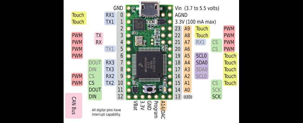
the 8-pin header (OLED header) brings out the full set of SPI signals, ie incl. MISO/DIN (Teensy pin #12), which isn’t needed for the display and DAC; in theory though, any other/any SPI device(s) might thus be attached instead (ie other than the OLED): ADCs, port expanders, etc., as happened, for example, here, using an atmega328 as a SPI slave. a variation of this uses two MCP23S17s and illuminated tact switches. or pots be used instead of the encoders (more details re available pins below). the board could also be mounted vertically, as a 4-6HP module: there’s two mounting holes.
disclaimer
- the circuit diagram was drawn by hand (which is to say, in pcb-view); the schematic (rev 2e) is entirely post-hoc, though it should be (is) a fairly accurate reflection of what’s going on. anyways, it’s all generic digital module stuff, so fairly unexciting. here’s the basics, more verbose (this pertains to 2d, 2e boards):
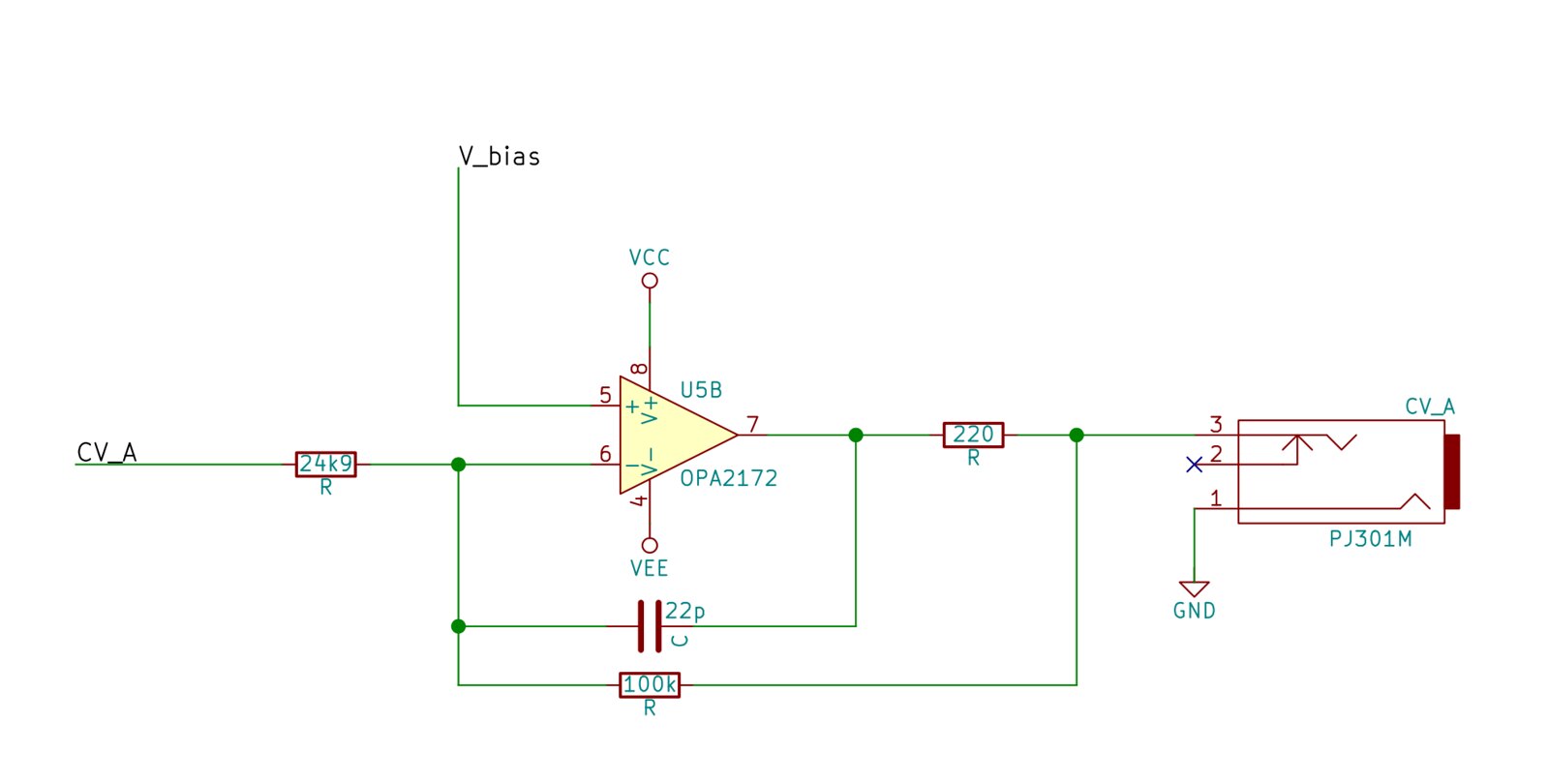
CV outputs:
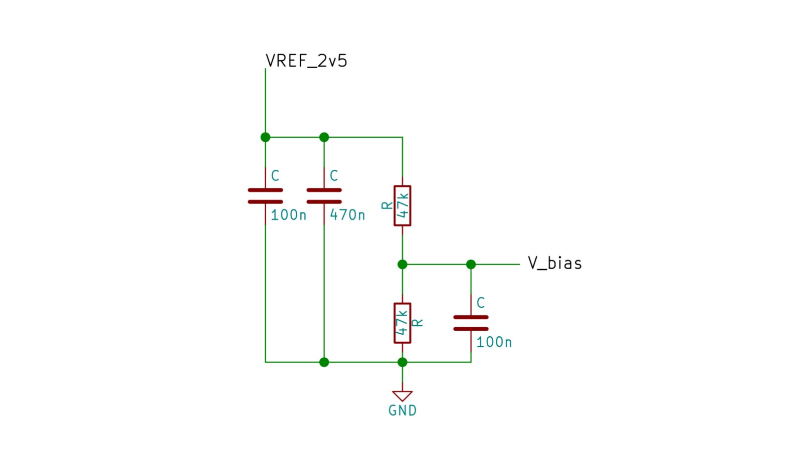
- inverting op amp, -4x gain and offset (V_bias = 1.25v):
-
V_ref/2 is formed by a voltage divider (the two 47k resistors marked with a
*) and the DAC reference (2.5v), so V_bias = 1.25v. this will result in an output range from -3.75v (min) to +6.25v (max), or -3v to +6v in terms of the calibration points:V_out = - gain * V_dac + (gain + 1) * V_bias -
if you’d prefer a different range, you’ll have to change the bias voltage, or the divider, for that matter. for instance, changing the input resistor (see below) to 22k results in V_bias = 1.703v (= 47k / (47k + 22k) * 2.5v). the resulting range will be more like -1.5v to +8.5v (or -1v to +8v in terms of the calibration points).
-
should you prefer a fully positive output range (0v - 9v), a voltage divider formed from 15k and 47k should do the job: V_bias ~ 1.896v. (the firmware won’t know, of course, and not reflect those shifted ranges; you’ll have to recompile the code with
IO_10Venabled (see OC_options.h)). (Note this assumes 0v/9v on the inputs, too. (see below)). -
should you prefer 1.2V/OCT outputs, simply increase the output gain (namely, to -4.8). take a look at the “Dual CV Polymorpher Model 2OC” to see how that would be done. briefly: replace the 100k resistors in the feedback path with 120k . the resulting output range will be -4.7v / +7.27v, which, in theory, should do but isn’t entirely ideal because a) it leaves little headroom for calibration (ie at 7.200V), and b) the negative voltages might, in fact, damage certain Buchla modules. So, better to increase V_bias, too. In light of caveat b) above, you’ll want to make sure the adjusted range is mostly positive, but some headroom below 0V will be required for tuning the 0.000V calibration point correctly. to actually use this, recompile the code with
BUCHLA_4Uenabled (see OC_options.h)).
CV inputs:
- inverting op amp with negative offset (-5V), via AREF (LM4040-5):
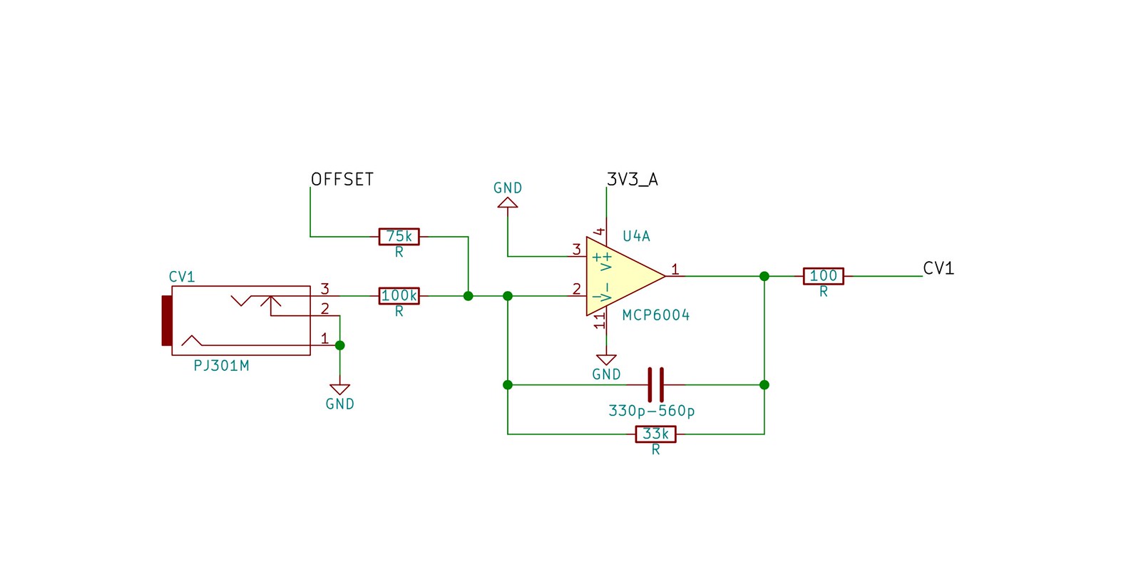
- the offset is ~ 6/9 of the ADC range (3.3v) or ~2.2v, so the inputs will match the DAC output range (-3v/6v).
- the range can be adjusted (should you prefer) by substituting the 75k resistor: 100k will yield a fully bipolar range (-5v/5v), 49k9 will yield ~ 0-10v.
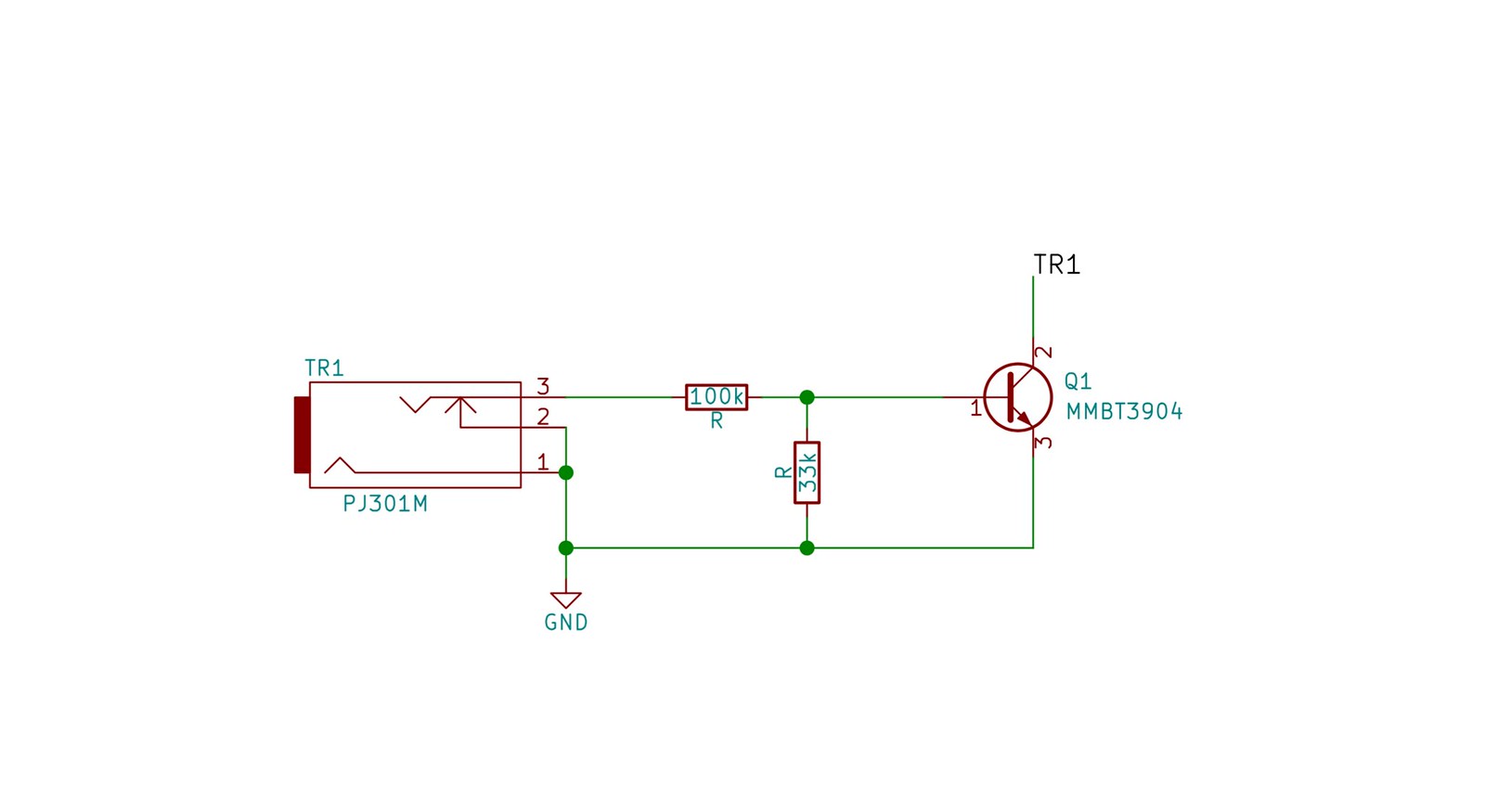
digital inputs:
- wired as (NPN) transistor ‘switches’. ie collector tied to 3V3 via a series resistor; emitter to ground; the trigger signals go into the base via a 100k series resistor and 33k to ground.
- as of rev 2.c the internal pull-up resistors are used (50k, ish):
encoders:
- the encoders use pins 14, 15, 16 resp. 21, 22, 23 (any or all of these pins could be wired as/to potentiometers); the two tact switches use pins 4 and 5. here’s the teensy pinout for reference: